

Custom Modules
With our standard products, Insight SIP’s aim is to offer certified, fully integrated modules covering a wide range of popular radio technologies. Our modules require only power to be functional radio nodes transmitting over the air and customer applications require only connecting peripheral devices for standalone products, or integrating the module into a more complex system via digital connections.
However sometimes customers have specific requirements, where they require additional features or functions to be integrated into a single module. Examples could include:-
- Combining multiple radios and antennas in a single device
- Developing a module for a custom radio device
- Integrating a customer designed ASIC with a standard radio
- Integrating sensors and peripherals into a single device
- Developing a module with a specific radio device not currently offered by Insight SIP
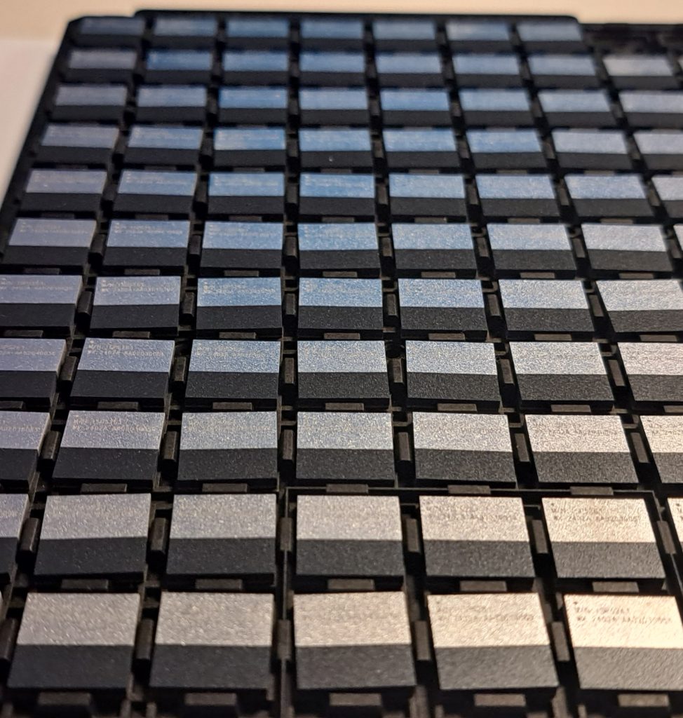
In such cases, it is possible for Insight SIP to design a SIP to the customers own specification. Such a device could be an adaption or combination of technologies already offered in our standard product range, or a completely new “clean sheet” design starting from scratch.
Design Process
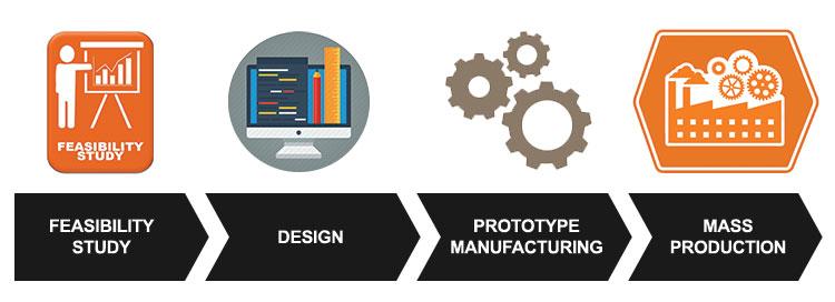
The starting point for a SIP design would usually be a reference design of the desired solution, and a working prototype on a standard PCB. A target size, form factor, and required external connections for the custom SIP would also be specified at this point.
From here, the first step would be to identify suitable components, and investigate in what packages they are available (WLCSP/Flipchip/0105 etc. depending on component type). Clearly for a miniature SIP, it is preferable to have components in small form factors wherever possible.
Once a precise BOM is defined, an initial floor plan can be created, defining the component layout and interconnection technology. This might include stacked semiconductors, wire bonding, flip-chip, depending on the precise project requirements. If the design requires an integrated antenna, then space and position will be allocated for this element.
The next stage is the most crucial of the SIP design process – the detailed design. Here Insight SIP applies its unique methodology that integrates physical layout with electromagnetic simulation to ensure the highest performance level.
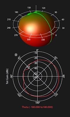
Alongside this the antenna will be designed. Insight SIP’s unique “Antenna in Package” approach means the antenna is simulated as part of the whole package, leading to optimum performance and omnidirectional radiation pattern. Where applicable, Insight SIP will draw on its library of antenna designs which cover the range from 1 – 8 Ghz, to speed up the design process and minimize risk.
Historically, we have carried out designs using different materials such as LTCC and IPD; however today these tend to be only used in some specific niches and the vast majority of designs use high quality laminate substrates.
Once the design is complete prototypes will be built and tested. The comprehensive design process means that prototypes can be expected to be functional on the first pass. A second design pass will normally be carried out to fully optimize the design and performance.
The final steps of the process are full industrialization and radio certification to enable mass production to start.
Advantages of a custom SIP
The key advantages of a custom SIP are as follows
- Unique product that matches customer’s exact requirements.
- Miniature integrated device that will allow the component to be used in the smallest form factor applications.
- High quality and repeatable manufacturing process leading to consistently performing products
- Capacity for very high volume production with OSATs (SIP manufacturers).
- Physically robust product due to overmolded design
- Fully certified “ready to go” device for use in customer applications
Points to consider with a custom SIP
The following are points to bear in mind when considering a custom SIP design.
- Whilst the ultimate mass production cost of a custom SIP is not significantly different from that using a traditional PCB approach, the design cycle is inevitably longer and more expensive.
- Changes to the SIP design are more complex and time consuming so a stable reference design is a pre-requisite
- In addition to design costs, there may be NRE costs associated with manufacturing set up.
- Due to there being a more limited set of possible subcontractors, the SIP approach is not well adapted to lower volume production, in most cases.
For more information please contact us with your requirements.